Micro-Flip Chip BGA
Case study – Manufacturing of a micro-FCBGA with 2100 connections and a pitch of 150µm
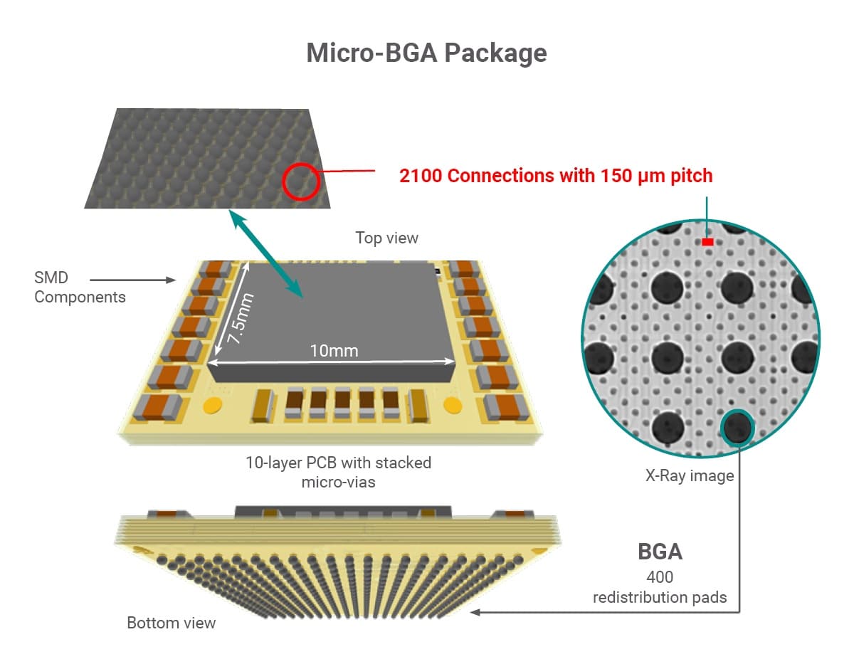
Packing more circuitry in always smaller component packages is a trend that requires microelectronic design and assembly expertise as well as highest accuracy. Micro-Flip Chip Ball Grid Array (Micro-FCBGA) is a case in point. This assembly technique that allows to meet the demand for low size and weight packages with high-density interconnects is quite challenging to perform. Ultra-fine pitch FCBGAs require very high precision to guarantee the reliability of the many interconnections. In this case study, we will outline how Valtronic developed a process for the assembly of a customized Micro-FCBGAs with 2100 connections and a pitch of 150µm.
A challenging micro-FCBGA project

Our customer approached Valtronic with very specific requirements for the assembly of a Micro-BGA package. A quite challenging project as 2100 bump connections on a die measuring 7.5mm x 10mm had to be attached and connected to a PCB with as many tiny connection pads. With a pitch as small as 150µm, placement accuracy and reflow management are key for the successful manufacturing of such highly customized packages.
Extreme accuracy of placement
Flipping the chip and accurately placing the 2100 bumps on their pads is key. It requires the right equipment and experience with such tiny components. Below, we share with you some tips regarding the steps and what you should focus on to succeed.
Placement tolerance
The placement tolerance for such a highly miniaturized component is ±10µm for maximum mechanical contact and minimal assembly defects. An accuracy we could reach thanks to our state-of the art Flip Chip assembly equipment and the know-how of our experienced team.
Solder paste stencil design
The solder paste stencil is an essential component for the successful placement of such a Micro-FCBGA. Printing the right stencil allows to control the amount of solder paste deposited and to obtain the optimal release behavior. To design and print such a customized and state-of-the-art stencil for fine-pitch and ultrafine-pitch surface-mount assembly, it is indispensable to master the latest stencil technologies and advances.
Our recommendation
Control your PCBs before ordering your paste stencils to adjust the stencil openings file if necessary
To make sure the PCB pads and the bumps will fit perfectly, it is preferable to first get the PCBs before cutting the stencils. From the Gerber file to manufacturing, PCBs can be subject to shrinking and stretching. In this case study, the PCB was designed and delivered by our customer. To make sure the stencil would perfectly match with the PCB pads, a PCB control was performed at reception before ordering the stencils. This allowed to perform an adjustment to the stencil opening file.
Solder reflow process
The reliability of a Micro-BGA package is also very dependent on the reflow soldering process. An inappropriate reflow profile can indeed lead to many defects such as voids, i.e. cavities formed in the solder joint. Solder joint reliability between the component and the board is crucial, even more with finer pitches and smaller solder sphere volumes. Voids reduce the mechanical robustness of the board level interconnection and thus also the conducting performance of the solder joint. For this project, we used a solder paste of Class 5. To obtain the perfect reflow, it is key to have experience with the different standard processes and with the types of ROHs solder pastes. Reflow processes however will have to be adapted according to the PCB type and shape. Here again, long experience in microelectronic assembly allows for quick and optimized fine-tuning of all the reflow parameters.
Underfill
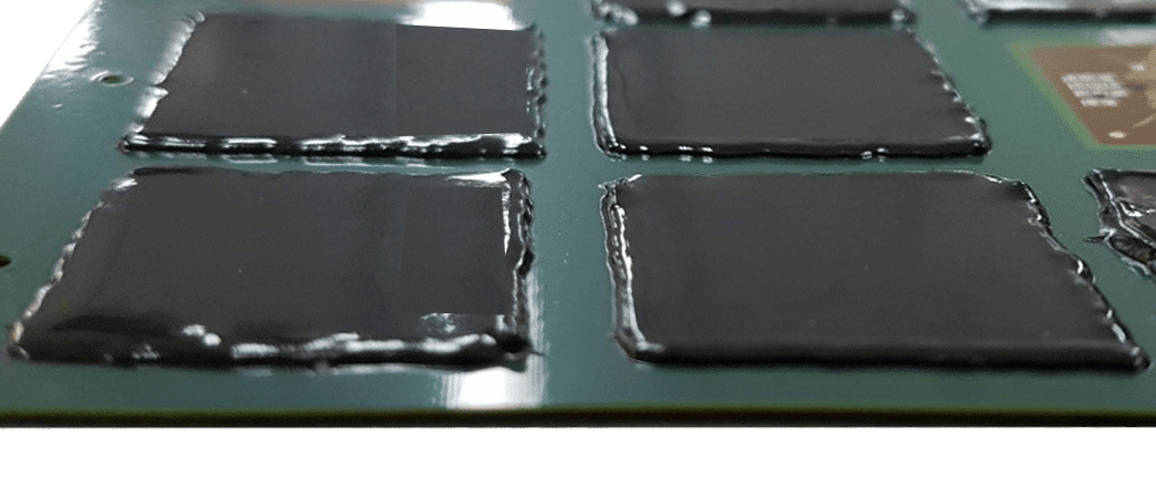
Underfill encapsulation allows to mechanically couple the chip and the substrate with the aim to reduce stress to the solder bumps and improve the reliability of the solder joints. The underfill operation has to be even more accurate with such miniaturized packages which offer limited access for the dispensing operation. Underfill material viscosity, surface tension, and contact angle are key properties to consider for an optimized gap filling process and are to be chosen and adapted according to the PCB type and morphology. For this specific Micro-FCBGA, we used a low-viscosity epoxy resin which was dispensed in an L-Shape pattern. This allowed us to obtain excellent results as confirmed by acoustic microscope examination.
Identification & Qualification of Critical SuppliersIdentification and qualification of critical suppliers is key to maintain the reliability and stability of the process.

Glob-Top Encapsulation
For the encapsulation we used a high-viscosity dam resin and a low-viscosity resin for the fill. In the encapsulation step, expertise and deep experience with the different resin-types allows to set up a series of validated processes allowing for reduced shrinkage during curing. Still, adjustments always need to be made according to each product. The bigger the surface to be filled, the higher the risk of stress during curing and thus of PCB deformation and damaged connections.
X-Ray Inspection
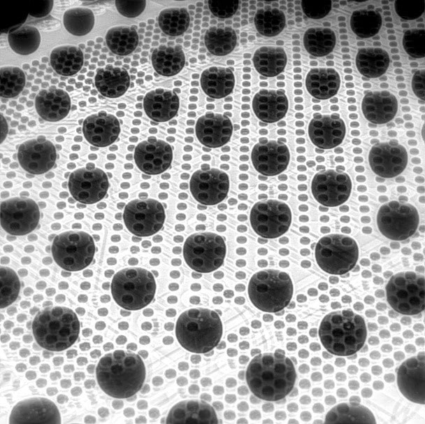
In customized packaging such as this micro-FCBGA solder connections to the PCB are hidden from view and cannot be inspected with traditional microscopes. X-Ray inspection is essential and required to check for voiding and connection quality. In terms of voiding, the results were in conformity with the IPC requirements. The inspection also confirmed high quality for the 2100 connections between chip and substrate.

A customized high-density package with surface-mount compatibility
Although highly customized and complex, this high-density package can be placed on any standard circuit board thanks to a redistribution layer of 400 pads. The whole process has been qualified which ensures for the sustained high-quality manufacturing of this Micro-FCBGA. This customized process can serve as a basis for further high-density packaging customization.
High-density packaging customization – More is possible
The challenge of this project was limited to one single die to attach to a PCB. The 2100 pads were successfully soldered to the PCB. Expertise in and experience with different assembly technologies would allow to push the challenge even further. Several dies could be stacked and interconnected to this PCB for even more embedded functionalities. Valtronic has the expertise and state-of-the-art equipment to meet such challenging projects. For over 35 years, our team has been delivering high-quality products to our customers in the advanced industrial industry and in the stringent medical industry.
- High interconnection density
- Best I/O density for a given PCB area
- Reduced footprint
- Reduced electrical resistance
- Preserved electrical signal integrity
- Better heat dissipation
- Increased speed of IC
- Can be supported with standard assembly equipment
- More prone to stress because of flexural stress from the circuit board and thermal expansion mismatches leading to potential reliability issues
- Inspecting of solder balls and solder joints for defects requires X-Ray inspection once the BGA has been soldered onto the circuit board
- Microprocessors/
microcontrollers - ASICs
- Memory
Medical:
- Imaging
- Active implants
- Ultrasonic probes
- Endoscopy
Next Issue of the Valtronicles
Placement of the tiniest components – 008004
Sign Up Now
to get informed about the next issues of the Valtronicles


